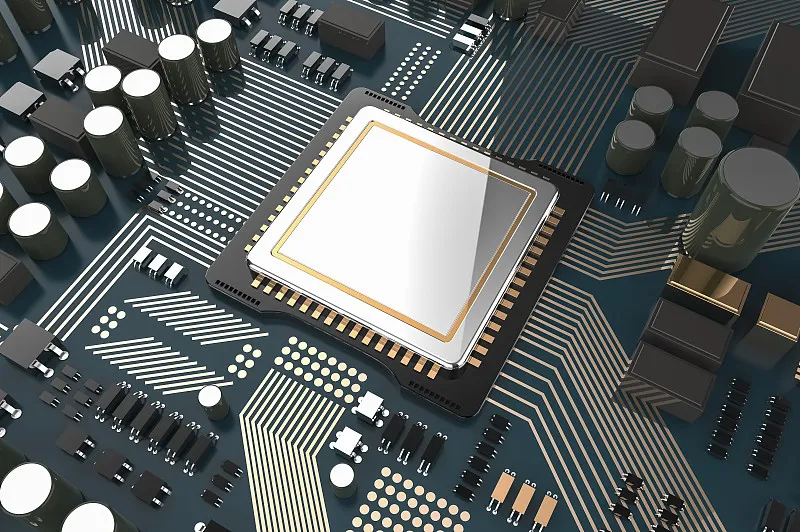
Chip packing is the term for materials that hold semiconductors. Encapsulation is the process of wrapping circuit components in an enclosure to prevent physical damage or corrosion. It also makes it possible to attach electrical contacts that are connected to printed circuit boards.
The shell that is used to install semiconductor integrated circuit chips plays a crucial role in various aspects, such as placing, fixing, sealing, protecting the chip, and improving its thermal performance. It serves as a connection between the internal world of the chip and the external circuits. The contacts on the chip are connected to the pins of the packaging shell through wires, which, in turn, are connected with other devices through wires on the printed circuit board. Therefore, packaging plays a significant role in both CPU and other LSI integrated circuits.
 Common types of chip packaging
Common types of chip packaging
- DIP dual inline
DIP (Dual Inline in Package) refers to an integrated circuit chip that is packaged in a dual inline format. The vast majority of small and medium-sized integrated circuits (ICs) use this packaging format, with a general number of pins not exceeding 100. CPU chips packaged with DIP have two rows of pins that need to be inserted into chip sockets with a DIP structure. Of course, it can also be directly inserted into circuit boards with the same number of solder holes and geometric arrangements for welding. Special care should be taken when inserting and unplugging DIP packaged chips from the chip socket to avoid damaging the pins.
Features:
1) Suitable for punching and welding on PCB (printed circuit board), easy to operate.
2) The ratio between packaging area and chip area is large, so the volume is also large. The 8088 in the Intel series CPU adopts this packaging form, as well as cache and early memory chips.
- Component encapsulated
The distance between chip pins in PQFP (Plastic Quad Flat Package) packaging is very small, and the pins are very thin. Generally, large-scale or ultra-large integrated circuits use this packaging form, with several pins generally exceeding 100. The chips packaged in this form must be soldered together with the motherboard using SMD (Surface Mount Device Technology). Chips installed using SMD do not need to be punched on the motherboard, as there are generally designed solder joints for the corresponding pins on the surface of the motherboard. Align each pin of the chip with the corresponding solder joint to achieve welding with the motherboard. The chip soldered on using this method is difficult to disassemble without special tools.
The chips packaged in PFP (Plastic Flat Package) mode are the same as those packaged in PQFP mode. The only difference is that PQFP is generally square, while PFP can be either square or rectangular.
Features:
1) Suitable for SMD surface mount technology installation and wiring on PCB circuit boards.
2) Suitable for high-frequency use.
3) Easy to operate and high reliability.
4) The ratio between the chip area and the packaging area is relatively small.
The Intel series CPUs, including the 80286, 80386, and some 486 motherboards, use this packaging form.
3. PGA pin net format
The PGA (Pin Grid Array Package) chip packaging consists of multiple square array pins inside and outside the chip. Each square array pin is placed at a certain distance along the circumference of the chip. Depending on the number of pins, they can be enclosed in 2-5 circles. You need to insert the chip into a dedicated PGA socket to install it. The CPU socket named ZIF was introduced with the 486 chip. It’s specifically designed to meet PGA-packaged CPUs’ installation and disassembly requirements.
Features:
1) The insertion and removal operation is more convenient and highly reliable.
2) It can adapt to higher frequencies. The PGA packaging form is used by the Intel series CPU, the 80486, and Pentium, as well as the Pentium Pro.
4. BGA ball grid array type
BGA packaging technology can be divided into five categories:
1) PBGA (Plastic BGA) substrate: This is generally a multi-layer board made up of 2-4 layers of organic materials. The Pentium II, III, and IV processors in the Intel series of CPUs all adopt this packaging form.
2) CBGA (Ceramic BGA) substrate: This refers to a ceramic substrate, and the electrical connection between chips and substrates is usually installed using FlipChip (FC). The Pentium I, II, and Pentium Pro processors in the Intel series of CPUs have all adopted this packaging form.
3) FCBGA (FilpChipBGA) substrate: This is a hard multilayer substrate.
4) TBGA (TapeBGA) substrate: The substrate is a ribbon-soft 1-2 layer PCB circuit board.
5) CDPBGA (Carity Down PBGA) substrate: This refers to the chip area (also known as the cavity area) with a square depression in the packaging center.
Features:
1) Although the number of I/O pins has increased, the distance between pins is much greater than that of QFP packaging, which improves the yield.
2) The power consumption of BGA increases, but the use of controllable collapse chip welding can improve the electric heating performance.
3) The signal transmission delay is small, and the adaptive frequency is greatly increased.
4) The assembly can be coplanar welded, greatly improving reliability.
Chip packaging is crucial to protect chips from external environmental influences. Chips are very fragile and susceptible to external environmental influences such as temperature, humidity, dust, and static electricity. If the chip is not packaged, it will easily be affected by these factors, leading to damage or failure of the chip. Therefore, chip packaging provides the necessary protection to ensure the long-term stability and reliability of the chip. Chip packaging also provides necessary electrical and mechanical connections. The chip needs to be connected to other electronic components to achieve the functionality of the circuit.
Article Source: KSPCBA BLOG